Powerful bipolar transistor amplifier circuit. Do-it-yourself class A transistor amplifier. Two-stage transistor amplifier
There were already publications on Habré about DIY tube amplifiers, which were very interesting to read. No doubt, they sound wonderful, but for everyday use it is easier to use a transistor device. Transistors are more convenient because they do not require warming up before operation and are more durable. And not everyone dares to start a lamp saga with anode potentials under 400 V, and transistor transformers for a couple of tens of volts are much safer and simply more affordable.
I chose John Linsley Hood's 1969 circuit as the circuit to reproduce, taking the author's parameters based on the impedance of my speakers 8 ohms.
The classic scheme from a British engineer, published almost 50 years ago, is still one of the most reproducible and collects about itself exclusively positive reviews. There are many explanations for this:
- the minimum number of elements simplifies installation. It is also believed that the simpler the design, the better sound;
- despite the fact that there are two output transistors, they do not need to be sorted into complementary pairs;
- output of 10 watts with a margin is enough for ordinary human dwellings, and an input sensitivity of 0.5-1 volts is very well consistent with the output of most sound cards or players;
- class A - it is also class A in Africa, if we are talking about good sound. About comparison with other classes will be a little lower. 
Internal design
The amplifier starts with power. Separation of two channels for stereo is best done from two different transformers, but I limited myself to one transformer with two secondary windings. After these windings, each channel exists on its own, so we must not forget to multiply by two everything mentioned below. On the breadboard we make bridges on Schottky diodes for the rectifier.
It is possible on ordinary diodes or even ready-made bridges, but then they need to be shunted with capacitors, and the voltage drop across them is greater. After the bridges, there are CRC filters of two 33,000 microfarad capacitors and a 0.75 ohm resistor between them. If you take both the capacitance and the resistor less, then the CRC filter will become cheaper and heat up less, but the ripple will increase, which is not comme il faut. These parameters, IMHO, are reasonable in terms of price-effect. A powerful cement resistor is needed in the filter, with a quiescent current of up to 2A it will dissipate 3 W of heat, so it is better to take it with a margin of 5-10 W. For the rest of the resistors in the power circuit, 2 W will be enough.
Next, we move on to the amplifier board itself. A lot of ready-made kits are sold in online stores, but there are no less complaints about the quality of Chinese components or illiterate layouts on the boards. Therefore, it is better to do it yourself, under your own “loose”. I made both channels on a single breadboard, so that later I can attach it to the bottom of the case. Run with test items:

Everything except the output transistors Tr1/Tr2 is located on the board itself. Output transistors are mounted on radiators, more on that below. To the author's scheme from the original article, you need to make the following remarks:
Not everything needs to be soldered right away. It is better to put resistors R1, R2 and R6 first with trimmers, after all the adjustments, unsolder them, measure their resistance and solder the final fixed resistors with the same resistance. The setting is reduced to the following operations. First, using R6, it is set so that the voltage between X and zero is exactly half of the voltage + V and zero. In one of the channels, I lacked 100 kOhm, so it's better to take these trimmers with a margin. Then, with the help of R1 and R2 (keeping their approximate ratio!) the quiescent current is set - we put the tester to measure direct current and measure this very current at the input point of the plus supply. I had to significantly reduce the resistance of both resistors to get desired current rest. The quiescent current of the amplifier in class A is maximum and, in fact, in the absence of an input signal, everything goes into thermal energy. For 8 ohm speakers, this current, according to the author's recommendation, should be 1.2 A at 27 volts, which means 32.4 watts of heat per channel. Since it can take several minutes for the current to be applied, the output transistors must already be on cooling heatsinks or they will quickly overheat and die. Because they get hot most of the time.
It is possible that, as an experiment, you will want to compare the sound of different transistors, so you can also leave the possibility of a convenient replacement for them. I tried on the input 2N3906, KT361 and BC557C, there was a slight difference in favor of the latter. In the pre-weekend, we tried KT630, BD139 and KT801, settled on imported ones. Although all of the above transistors are very good, and the difference can be rather subjective. At the output, I immediately put 2N3055 (ST Microelectronics), since many people like them.
When adjusting and lowering the resistance of the amplifier, the cutoff frequency of the low frequencies may increase, so for the capacitor at the input it is better to use not 0.5 microfarads, but 1 or even 2 microfarads in a polymer film. The Russian picture-scheme “Ultralinear Class A Amplifier” is still circulating on the Web, where this capacitor is generally proposed as 0.1 microfarads, which is fraught with a cutoff of all basses at 90 Hz:

They write that this circuit is not prone to self-excitation, but just in case, a Zobel circuit is placed between the X point and the ground: R 10 Ohm + C 0.1 microfarad.
- fuses, they can and should be installed both on the transformer and on the power input of the circuit.
- it would be very appropriate to use thermal paste for maximum contact between the transistor and the heatsink.
Locksmith and carpentry
Now about the traditionally most difficult part in DIY - the case. The dimensions of the case are set by radiators, and in class A they should be large, remember about 30 watts of heat on each side. At first, I underestimated this power and made a case with average radiators 800cm² per channel. However, with a set quiescent current of 1.2A, they heated up to 100 ° C in just 5 minutes, and it became clear that something more powerful was needed. That is, you need to either install larger radiators, or use coolers. I didn’t want to make a quadcopter, so I bought giant handsome HS 135-250s with an area of 2500 cm² for each transistor. As practice has shown, such a measure turned out to be a little redundant, but now the amplifier can be safely touched by hands - the temperature is only 40 ° C even in rest mode. Drilling holes in the radiators for fasteners and transistors became some problem - the originally purchased Chinese metal drills were drilled extremely slowly, it would take at least half an hour for each hole. Cobalt drills with a sharpening angle of 135 ° from a well-known German manufacturer came to the rescue - each hole is passed in a few seconds!I made the body out of Plexiglas. We immediately order cut rectangles from glaziers, make the necessary holes for fastenings in them and paint the reverse side with black paint.


The plexiglass painted on the back looks very nice. Now it remains only to assemble everything and enjoy the music ... oh yes, during the final assembly, it is also important to properly dilute the ground to minimize the background. As it was found out decades before us, C3 needs to be connected to the signal ground, i.e. to the minus of the input-input, and all other minuses can be sent to the "star" near the filter capacitors. If everything is done correctly, then no background can be heard, even if you bring your ear to the speaker at maximum volume. Another "ground" feature that is typical for sound cards that are not galvanically isolated from the computer is interference from the motherboard, which can creep through USB and RCA. Judging by the Internet, the problem is common: in the speakers you can hear the sounds of the HDD, printer, mouse and the background of the system unit's power supply. In this case, the easiest way is to break the ground loop by taping the ground on the amplifier plug with electrical tape. There is nothing to fear here, because. there will be a second ground loop through the computer.
I didn’t make a volume control on the amplifier, because I couldn’t get any high-quality ALPS, and I didn’t like the rustling of Chinese potentiometers. Instead, a conventional 47 kΩ resistor was installed between the “ground” and the “signal” of the input. Moreover, the regulator of the external sound card always at hand, and each program also has a slider. Only the vinyl player does not have a volume control, so to listen to it, I attached an external potentiometer to the connecting cable.

I can guess this container in 5 seconds...
Finally, you can start listening. Sound source is Foobar2000 → ASIO → external Asus Xonar U7. Speakers Microlab Pro3. The main advantage of these speakers is a separate block of their own amplifier on the LM4766 chip, which can be immediately removed somewhere far away. Much more interesting with this acoustics sounded the amplifier from the Panasonic mini-system with the proud inscription Hi-Fi or the amplifier of the Soviet player Vega-109. Both of the above devices work in class AB. The JLH presented in the article outplayed all of the above comrades in one wicket, according to the results of a blind test for 3 people. Although the difference was audible to the naked ear and without any tests, the sound is clearly more detailed and transparent. It's quite easy, for example, to hear the difference between 256kbps MP3 and FLAC. I used to think that the lossless effect is more like a placebo, but now the opinion has changed. Similarly, it became much more pleasant to listen to files not compressed from loudness war - dynamic range less than 5 dB is not ice at all. The Linsley Hood is worth the time and money, as a similar branded amp will cost a lot more.Material costs
Transformer 2200 rub.Output transistors (6 pieces with a margin) 900 rubles.
Filter capacitors (4 pcs) 2700 r.
"Rose" (resistors, small capacitors and transistors, diodes) ~ 2000 rubles.
Radiators 1800 r.
Plexiglas 650 rub.
Paint 250 rub.
Connectors 600 rub.
Boards, wires, silver solder, etc. ~1000 r.
TOTAL ~12100 rub.
The transistor amplifier, despite its already long history, remains a favorite subject of study for both beginners and venerable radio amateurs. And this is understandable. He is an indispensable integral part the most massive and amplifiers of low (sound) frequency. We will look at how the simplest transistor amplifiers are built.
Amplifier frequency response
In any television or radio receiver, in every music center or a sound amplifier, you can find transistor sound amplifiers (low frequency - LF). The difference between audio transistor amplifiers and other types lies in their frequency response.
The transistor audio amplifier has a uniform frequency response in the frequency band from 15 Hz to 20 kHz. This means that all input signals with a frequency within this range are converted (amplified) by the amplifier in approximately the same way. The figure below shows the ideal frequency response curve for an audio amplifier in the coordinates "amplifier gain Ku - input signal frequency".
This curve is almost flat from 15 Hz to 20 kHz. This means that such an amplifier should be used specifically for input signals with frequencies between 15 Hz and 20 kHz. For input signals above 20 kHz or below 15 Hz, the efficiency and quality of its performance rapidly decrease.
The type of frequency response of the amplifier is determined by the electrical radio elements (ERE) of its circuit, and above all by the transistors themselves. An audio amplifier based on transistors is usually assembled on the so-called low- and mid-frequency transistors with a total bandwidth of input signals from tens and hundreds of Hz to 30 kHz.
Amplifier class
As you know, depending on the degree of continuity of the current flow throughout its period through the transistor amplifying stage (amplifier), the following classes of its operation are distinguished: "A", "B", "AB", "C", "D".
In the class of operation, current "A" flows through the stage for 100% of the period of the input signal. The operation of the cascade in this class is illustrated in the following figure.

In the class of operation of the amplifier stage "AB", the current flows through it for more than 50%, but less than 100% of the period of the input signal (see figure below).

In the class of operation of the "B" stage, the current flows through it exactly 50% of the period of the input signal, as illustrated in the figure.

And finally, in the class of operation of the "C" stage, the current through it flows less than 50% of the period of the input signal.
Low-frequency amplifier on transistors: distortion in the main classes of work
In the working area, a class "A" transistor amplifier has a low level of non-linear distortion. But if the signal has impulse surges in voltage, leading to saturation of the transistors, then higher harmonics (up to the 11th) appear around each “standard” harmonic of the output signal. This causes the phenomenon of the so-called transistorized or metallic sound.
If low-frequency power amplifiers on transistors have an unstabilized power supply, then their output signals are modulated in amplitude near the mains frequency. This leads to harshness of the sound at the left edge of the frequency response. Various methods of voltage stabilization make the design of the amplifier more complex.
The typical efficiency of a single-ended class A amplifier does not exceed 20% due to the always-on transistor and the continuous flow of the DC component. You can make a class A amplifier push-pull, the efficiency will increase slightly, but the half-waves of the signal will become more asymmetric. The transfer of the cascade from the work class "A" to the work class "AB" quadruples the nonlinear distortion, although the efficiency of its circuit increases.
In amplifiers of classes "AB" and "B", distortion increases as the signal level decreases. You involuntarily want to turn up such an amplifier louder to complete the sensations of the power and dynamics of the music, but often this does not help much.
Intermediate classes of work
The class of work "A" has a variety - the class "A +". In this case, the low-voltage input transistors of the amplifier of this class operate in class "A", and the high-voltage output transistors of the amplifier, when their input signals exceed a certain level, go into classes "B" or "AB". The efficiency of such cascades is better than in the pure class "A", and the non-linear distortion is less (up to 0.003%). However, their sound is also "metallic" due to the presence of higher harmonics in the output signal.
For amplifiers of another class - "AA" the degree of nonlinear distortion is even lower - about 0.0005%, but higher harmonics are also present.
A return to a class "A" transistor amplifier?
Today, many experts in the field of high-quality sound reproduction advocate a return to tube amplifiers, since the level of non-linear distortion and higher harmonics introduced by them into the output signal is obviously lower than that of transistors. However, these advantages are largely offset by the need for a matching transformer between the high-resistance tube output stage and the low-resistance ones. speakers. However, a simple transistorized amplifier can also be made with a transformer output, as will be shown below.
There is also a point of view that only a hybrid tube-transistor amplifier can provide the ultimate sound quality, all stages of which are single-ended, not covered and work in class "A". That is, such a power follower is an amplifier on a single transistor. Its scheme can have the maximum achievable efficiency (in class "A") no more than 50%. But neither the power nor the efficiency of the amplifier are indicators of the quality of sound reproduction. In this case, the quality and linearity of the characteristics of all EREs in the circuit are of particular importance.
Since single-ended circuits are gaining this perspective, we will look at their options below.
single-ended amplifier with one transistor
Its circuit, made with a common emitter and R-C connections for input and output signals for operation in class "A", is shown in the figure below.

It shows the npn transistor Q1. Its collector is connected to the +Vcc positive terminal via a current-limiting resistor R3, and its emitter is connected to -Vcc. transistor amplifier p-n-p structures will have the same circuit, but the power supply leads will be reversed.
C1 is a decoupling capacitor by which the AC input source is separated from the DC voltage source Vcc. At the same time, C1 does not prevent the passage of an alternating input current through the base-emitter junction of transistor Q1. Resistors R1 and R2, together with the resistance of the "E - B" junction, form Vcc to select the operating point of the transistor Q1 in static mode. Typical for this circuit is the value of R2 = 1 kOhm, and the position of the operating point is Vcc / 2. R3 is a load resistor of the collector circuit and serves to create on the collector AC voltage output signal.
Assume that Vcc = 20 V, R2 = 1 kΩ, and the current gain h = 150. We select the emitter voltage Ve = 9 V, and the voltage drop at the E-B junction is Vbe = 0.7 V. This value corresponds to the so-called silicon transistor. If we were considering an amplifier based on germanium transistors, then the voltage drop across the open E-B junction would be Vbe = 0.3 V.
Emitter current, approximately equal to collector current
Ie = 9 V/1 kΩ = 9 mA ≈ Ic.
Base current Ib = Ic/h = 9 mA/150 = 60 µA.
Voltage drop across resistor R1
V(R1) = Vcc - Vb = Vcc - (Vbe + Ve) = 20V - 9.7V = 10.3V,
R1 \u003d V (R1) / Ib \u003d 10.3 V / 60 μA \u003d 172 kOhm.
C2 is needed to create a circuit for the passage of the variable component of the emitter current (actually the collector current). If it were not there, then the resistor R2 would severely limit the variable component, so that the bipolar transistor amplifier in question would have a low current gain.
In our calculations, we assumed that Ic = Ib h, where Ib is the base current flowing into it from the emitter and arising when a bias voltage is applied to the base. However, through the base always (both with and without bias) the leakage current from the collector Icb0 also flows. Therefore, the real collector current is Ic = Ib h + Icb0 h, i.e. the leakage current in the circuit with OE is amplified by 150 times. If we were considering an amplifier based on germanium transistors, then this circumstance would have to be taken into account in the calculations. The fact is that they have a significant Icb0 of the order of several μA. In silicon, it is three orders of magnitude smaller (about a few nA), so it is usually neglected in calculations.
Single ended amplifier with MIS transistor
Like any amplifier field effect transistors, the circuit under consideration has its own analogue among amplifiers. Therefore, we consider an analogue of the previous circuit with a common emitter. It is made with a common source and R-C connections for input and output signals for operation in class "A" and is shown in the figure below.

Here C1 is the same decoupling capacitor, by means of which the source of the alternating input signal is separated from the source of the constant voltage Vdd. As you know, any field-effect transistor amplifier must have the gate potential of its MIS transistors below the potentials of their sources. In this circuit, the gate is grounded by R1, which is typically high resistance (100 kΩ to 1 MΩ) so that it does not shunt the input signal. There is practically no current through R1, so the gate potential in the absence of an input signal is equal to the ground potential. The source potential is higher than the ground potential due to the voltage drop across the resistor R2. Thus, the gate potential is lower than the source potential, which is necessary for normal operation Q1. Capacitor C2 and resistor R3 have the same purpose as in the previous circuit. Since this is a common-source circuit, the input and output signals are out of phase by 180°.
Amplifier with transformer output
The third single-stage simple transistor amplifier, shown in the figure below, is also made according to the common emitter circuit for operation in class "A", but it is connected to a low-impedance speaker through a matching transformer.

The primary winding of the transformer T1 is the load of the collector circuit of the transistor Q1 and develops the output signal. T1 sends the output signal to the speaker and ensures that the output impedance of the transistor matches the low (on the order of a few ohms) speaker impedance.
The voltage divider of the collector power supply Vcc, assembled on resistors R1 and R3, provides the choice of the operating point of the transistor Q1 (supplying a bias voltage to its base). The purpose of the remaining elements of the amplifier is the same as in the previous circuits.
Push-Pull Audio Amplifier
Push-pull low-frequency amplifier on two transistors splits input frequency into two antiphase half-waves, each of which is amplified by its own transistor cascade. After such amplification, the half-waves are combined into a complete harmonic signal, which is transmitted to the speaker system. Such a conversion of the low-frequency signal (splitting and re-merging), of course, causes irreversible distortion in it, due to the difference in the frequency and dynamic properties of the two transistors of the circuit. These distortions reduce the sound quality at the output of the amplifier.
Push-pull amplifiers operating in class "A" do not reproduce complex audio signals well enough, since there is a continuous flow in their shoulders D.C. elevated size. This leads to asymmetry of the half-waves of the signal, phase distortions and, ultimately, to the loss of sound intelligibility. When heated, two powerful transistors double the signal distortion in the low and infra-low frequencies. But still, the main advantage of the push-pull circuit is its acceptable efficiency and increased output power.
A push-pull transistor power amplifier circuit is shown in the figure.

This is an amplifier for class "A", but class "AB" and even "B" can also be used.
Transformerless Transistor Power Amplifier
Transformers, despite the success in their miniaturization, are still the most bulky, heavy and expensive ERE. Therefore, a way was found to eliminate the transformer from the push-pull circuit by performing it on two powerful complementary transistors. different types(n-p-n and p-n-p). Most modern power amplifiers use this principle and are designed to operate in class "B". A diagram of such a power amplifier is shown in the figure below.

Both of its transistors are connected according to a common collector (emitter follower) circuit. Therefore, the circuit transfers the input voltage to the output without amplification. If there is no input signal, then both transistors are on the border of the on state, but they are turned off.
When a harmonic signal is input, its positive half-wave opens TR1, but translates pnp transistor TR2 is fully into cutoff mode. Thus, only the positive half-wave of the amplified current flows through the load. The negative half-wave of the input signal opens only TR2 and turns off TR1, so that the negative half-wave of amplified current is supplied to the load. As a result, a full power amplified (due to current amplification) sinusoidal signal is emitted at the load.
Single transistor amplifier
To assimilate the above, we will assemble a simple transistor amplifier with our own hands and figure out how it works.
As a load of a low-power transistor T of type BC107, we turn on headphones with a resistance of 2-3 kOhm, we supply the bias voltage to the base from a high-resistance resistor R* of 1 MΩ, which decouples an electrolytic capacitor C with a capacity of 10 μF to 100 μF, we include it in the base circuit T. Feed the circuit we will be from a 4.5 V / 0.3 A battery.

If resistor R* is not connected, then there is neither base current Ib nor collector current Ic. If the resistor is connected, then the voltage at the base rises to 0.7 V and the current Ib = 4 μA flows through it. The current gain of the transistor is 250, which gives Ic = 250Ib = 1 mA.
Having assembled a simple transistor amplifier with our own hands, we can now test it. Connect the headphones and place your finger on point 1 of the diagram. You will hear a noise. Your body perceives the radiation of the mains at a frequency of 50 Hz. The noise you hear from the headphones is this radiation, only amplified by the transistor. Let us explain this process in more detail. An AC voltage of 50 Hz is connected to the base of the transistor through capacitor C. The voltage at the base is now equal to the sum of the DC bias voltage (approximately 0.7 V) coming from the resistor R* and the finger AC voltage. As a result, the collector current receives an alternating component with a frequency of 50 Hz. This alternating current is used to move the diaphragm of the speakers back and forth at the same frequency, which means we can hear a 50Hz tone at the output.
Listening to the 50 Hz noise level is not very interesting, so you can connect low-frequency signal sources (CD player or microphone) to points 1 and 2 and hear amplified speech or music.
A low frequency amplifier (ULF) is such a device for amplifying electrical vibrations corresponding to the frequency range audible to the human ear, i.e. ULF should amplify in the frequency range from 20 Hz to 20 kHz, but some ULF can have a range up to 200 kHz. ULF can be assembled as an independent device, or used in more complex devices - TVs, radios, radios, etc.
The peculiarity of this circuit is that the 11th output of the TDA1552 microcircuit controls the operating modes - Normal or MUTE.

C1, C2 - bypass blocking capacitors, used to cut off the constant component of the sinusoidal signal. Electrolytic capacitors should not be used. It is desirable to place the TDA1552 chip on a heatsink using heat-conducting paste.
In principle, the presented circuits are bridge circuits, since there are 4 amplification channels in one TDA1558Q microassembly case, therefore pins 1 - 2, and 16 - 17 are connected in pairs, and they receive input signals from both channels through capacitors C1 and C2. But if you need an amplifier for four speakers, then you can use the circuit option below, although the power will be 2 times less per channel.
The basis of the design is the TDA1560Q class H microassembly. The maximum power of such a ULF reaches 40 W, with a load of 8 ohms. Such power is provided by an approximately doubled voltage due to the operation of the capacitors.

The output power of the amplifier in the first circuit assembled on the TDA2030 is 60W at a load of 4 ohms and 80W at a load of 2 ohms; TDA2030A 80W at 4 ohm load and 120W at 2 ohm load. The second circuit of the considered ULF is already with an output power of 14 watts.

This is a typical two-channel ULF. With a little piping of passive radio components on this chip, you can assemble an excellent stereo amplifier with an output power of 1 watt per channel.
Microassembly TDA7265 - is a fairly powerful two-channel hi-fi amplifier class AB in a typical Multiwatt package, the microcircuit has found its niche in high-quality stereo equipment, Hi-Fi class. Simple switching circuits and excellent parameters made the TDA7265 a perfectly balanced and excellent solution for building high-quality amateur radio equipment.
First, a test version was assembled on a breadboard exactly as per the datasheet on the link above, and successfully tested on S90 speakers. The sound is good, but something was missing. After some time, I decided to remake the amplifier according to the modified circuit.
The Micro Assembly is a class AB quad amplifier designed specifically for use in automotive audio applications. Based on this microcircuit, several high-quality ULF variants can be built using a minimum of radio components. The microcircuit can be advised to beginner radio amateurs for home assembly of various acoustic systems.
The main advantage of the amplifier circuit on this microassembly is the presence of four independent channels in it. This power amplifier works in AB mode. It can be used to amplify various stereo signals. If desired, you can connect to acoustic system vehicle or personal computer.
TDA8560Q is just a more powerful analogue of the TDA1557Q chip, widely known to radio amateurs. The developers only strengthened the output stage, thanks to which the ULF is perfect for a two-ohm load.
The LM386 micro-assembly is a ready-made power amplifier that can be used in low-voltage designs. For example, when powering the circuit from battery. LM386 has a voltage gain of about 20. But by connecting external resistances and capacitances, you can adjust the gain up to 200, and the output voltage automatically becomes equal to half the supply voltage.
Microassembly LM3886 is an amplifier High Quality with an output power of 68 watts into a 4 ohm load or 50 watts into 8 ohms. At the peak moment, the output power can reach a value of 135 watts. Applicable to the microcircuit wide range voltages from 20 to 94 volts. Moreover, you can use both bipolar and unipolar power supplies. The ULF harmonic coefficient is 0.03%. Moreover, this is over the entire frequency range from 20 to 20,000 Hz.

The circuit uses two ICs in a typical connection - KR548UH1 as a microphone amplifier (installed in the PTT) and (TDA2005) in a bridged connection as final amplifier(installed in the siren case instead of the original board). As an acoustic emitter, a modified alarm sipen with a magnetic head is used (piezo emitters are not suitable). Improvement consists in disassembling the siren and throwing out the native tweeter with an amplifier. Microphone - electrodynamic. When using an electret microphone (for example, from Chinese handsets), the connection point of the microphone with the capacitor must be connected to + 12V through a resistor ~ 4.7K (after the button!). The 100K resistor in the K548UH1 feedback circuit is better to put with a resistance of ~ 30-47K. This resistor is used to adjust the volume. It is better to install the TDA2004 chip on a small radiator.
To test and operate - with a radiator under the hood, and a tangent in the cabin. Otherwise, squealing due to self-excitation is inevitable. The trimmer resistor sets the volume level so that there is no strong sound distortion and self-excitation. With insufficient volume (for example, a bad microphone) and a clear margin of power of the emitter, you can increase the gain of the microphone amplifier by increasing the value of the trimmer in the feedback circuit several times (the one that is 100K according to the scheme). In a good way - we would need another primambas that does not allow the circuit to self-excite - some kind of phase-shifting chain or a filter for the excitation frequency. Although the scheme and without complications works fine
Amplifiers, the main purpose of which is to amplify the signal in terms of power, are called power amplifiers. As a rule, such amplifiers drive a low-impedance load, such as a loudspeaker.


voltage 3-18 V (nominal - 6 V) . The maximum current consumption is 1.5 A at a quiescent current of 7 mA (at 6 V) and 12 mA (at 18 V). Voltage gain 36.5 dB. at -1 dB 20 Hz - 300 kHz. Rated output power at 10% THD
temporarily turn off the soundtrack. You can double the output power of the TDA7233D when they are turned on according to the scheme shown in fig. 31.42. C7 prevents self-excitation of the device in the area
high frequencies. R3 is selected until an equal amplitude of the output signals is obtained at the outputs of the microcircuits.

Rice. 31.43. KR174UNZ 7
KR174UN31 is intended for use as output low-power household REA.
When the supply voltage changes from
2.1 to 6.6 V with an average current consumption of 7 mA (without an input signal), the voltage gain of the microcircuit varies from 18 to 24 dB.
The coefficient of non-linear distortion at an output power of up to 100 mW is not more than 0.015%, the output noise voltage does not exceed 100 μV. Input microcircuit 35-50 kOhm. load - not less than 8 ohms. Operating frequency range - 20 Hz - 30 kHz, limit - 10 Hz - 100 kHz. The maximum input signal voltage is up to 0.25-0.5 V.
Low frequency amplifiers (ULF) are used to convert weak signals predominantly in the audio range into more powerful signals acceptable for direct perception through electrodynamic or other sound emitters.
Note that high-frequency amplifiers up to frequencies of 10 ... 100 MHz are built according to similar schemes, the whole difference most often comes down to the fact that the values of the capacitances of the capacitors of such amplifiers decrease as many times as the frequency of the high-frequency signal exceeds the frequency of the low-frequency one.
A simple single transistor amplifier
The simplest ULF, made according to the scheme with a common emitter, is shown in Fig. 1. A telephone capsule was used as a load. The allowable supply voltage for this amplifier is 3 ... 12 V.
It is desirable to determine the value of the bias resistor R1 (tens of kΩ) experimentally, since its optimal value depends on the supply voltage of the amplifier, the resistance of the telephone capsule, and the transmission coefficient of a particular instance of the transistor.
Rice. 1. Scheme of a simple ULF on one transistor + capacitor and resistor.
To select the initial value of the resistor R1, it should be taken into account that its value should be about a hundred or more times greater than the resistance included in the load circuit. To select a bias resistor, it is recommended to connect in series a constant resistor with a resistance of 20 ... 30 kOhm and variable resistance 100 ... 1000 kOhm, after which, having applied to the input of the amplifier sound signal small amplitude, for example, from a tape recorder or player, by turning the knob variable resistor achieve the best signal quality at its highest volume.
The value of the capacitance of the transition capacitor C1 (Fig. 1) can be in the range from 1 to 100 microfarads: the greater the value of this capacitance, the lower frequencies the ULF can amplify. To master the technique of amplifying low frequencies, it is recommended to experiment with the selection of the values of the elements and the operating modes of the amplifiers (Fig. 1 - 4).
Improved Single Transistor Amplifier Options
Complicated and improved in comparison with the scheme in fig. 1 amplifier circuits are shown in fig. 2 and 3. In the diagram in fig. 2 amplification stage additionally contains a chain of frequency-dependent negative feedback(resistor R2 and capacitor C2), which improves the signal quality.

Rice. 2. Scheme of a single-transistor ULF with a chain of frequency-dependent negative feedback.
Rice. 3. A single-transistor amplifier with a divider to supply a bias voltage to the base of the transistor.

Rice. 4. Single transistor amplifier with automatic bias setting for the base of the transistor.
In the diagram in fig. 3, the bias to the base of the transistor is set more “rigidly” using a divider, which improves the quality of the amplifier when its operating conditions change. An “automatic” bias setting based on an amplifying transistor is used in the circuit in fig. 4.
Two-stage transistor amplifier
By connecting in series two simple amplification stages (Fig. 1), you can get a two-stage ULF (Fig. 5). The gain of such an amplifier is equal to the product of the gains of the individual stages. However, it is not easy to obtain a large stable gain with a subsequent increase in the number of stages: the amplifier will most likely self-excite.

Rice. 5. Scheme of a simple two-stage bass amplifier.
New developments of low-frequency amplifiers, the schemes of which are often given on the pages of magazines recent years, pursue the goal of achieving a minimum coefficient of non-linear distortion, increasing the output power, expanding the bandwidth of amplified frequencies, etc.
At the same time, when setting up various devices and conducting experiments, a simple ULF is often needed, which can be assembled in a few minutes. Such an amplifier should contain a minimum number of deficient elements and operate in a wide range of supply voltage and load resistance.
ULF circuit on field-effect and silicon transistors
A diagram of a simple low-frequency power amplifier with a direct connection between the cascades is shown in fig. 6 [Rl 3/00-14]. The input impedance of the amplifier is determined by the value of the potentiometer R1 and can vary from hundreds of ohms to tens of megohms. The output of the amplifier can be connected to a load with a resistance of 2 ... 4 to 64 ohms and higher.
With a high-resistance load, the KT315 transistor can be used as VT2. The amplifier is operable in the supply voltage range from 3 to 15 V, although its acceptable performance is maintained even when the supply voltage drops down to 0.6 V.
Capacitor C1 can be selected from 1 to 100 microfarads. In the latter case (C1 \u003d 100 μF), the ULF can operate in the frequency band from 50 Hz to 200 kHz and above.

Rice. 6. Scheme simple amplifier low frequency on two transistors.
The amplitude of the ULF input signal should not exceed 0.5 ... 0.7 V. The output power of the amplifier can vary from tens of mW to units of W, depending on the load resistance and the magnitude of the supply voltage.
Setting up the amplifier consists in selecting resistors R2 and R3. With their help, the voltage at the drain of the transistor VT1 is set, equal to 50 ... 60% of the voltage of the power source. Transistor VT2 must be installed on a heat sink plate (radiator).
Track-cascade ULF with direct connection
On fig. 7 shows a diagram of another outwardly simple ULF with direct connections between the cascades. This kind of communication improves frequency characteristics amplifier in the low-frequency region, the circuit as a whole is simplified.
Rice. 7. circuit diagram three-cascade ULF with direct connection between the cascades.
At the same time, the tuning of the amplifier is complicated by the fact that each amplifier resistance has to be selected individually. Roughly, the ratio of resistors R2 and R3, R3 and R4, R4 and R BF should be within (30 ... 50) to 1. Resistor R1 should be 0.1 ... 2 kOhm. The calculation of the amplifier shown in fig. 7 can be found in the literature, eg [P 9/70-60].
Schemes of cascade ULF on bipolar transistors
On fig. 8 and 9 show cascode ULF circuits on bipolar transistors. Such amplifiers have a rather high gain Ku. The amplifier in fig. 8 has Ku=5 in the frequency band from 30 Hz to 120 kHz [MK 2/86-15]. ULF according to the scheme in Fig. 9 with a harmonic coefficient of less than 1% has a gain of 100 [RL 3/99-10].

Rice. 8. Cascade ULF on two transistors with gain = 5.

Rice. 9. Cascade ULF on two transistors with gain = 100.
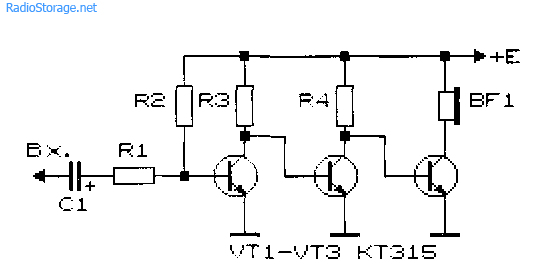
Economical ULF on three transistors
For portable electronic equipment, an important parameter is the efficiency of VLF. The scheme of such a ULF is shown in fig. 10 [RL 3/00-14]. Here, a cascade connection of a field-effect transistor VT1 and a bipolar transistor VT3 is used, and the transistor VT2 is turned on in such a way that it stabilizes the operating point of VT1 and VT3.
With an increase in the input voltage, this transistor shunts the emitter-base VT3 junction and reduces the value of the current flowing through the transistors VT1 and VT3.

Rice. 10. Scheme of a simple economical low-frequency amplifier on three transistors.
As in the above circuit (see Fig. 6), the input impedance of this ULF can be set in the range from tens of ohms to tens of megohms. A telephone primer, for example, TK-67 or TM-2V, was used as a load. A telephone capsule connected with a plug can simultaneously serve as a power switch for the circuit.
The ULF supply voltage ranges from 1.5 to 15 V, although the device remains operational even when the supply voltage drops to 0.6 V. In the supply voltage range of 2 ... 15 V, the current consumed by the amplifier is described by the expression:
1(µA) = 52 + 13*(Upit)*(Upit),
where Upit is the supply voltage in Volts (V).
If you turn off the transistor VT2, the current consumed by the device increases by an order of magnitude.
Two-cascade ULF with direct connection between the cascades
Examples of ULF with direct connections and a minimum selection of the operating mode are the circuits shown in Fig. 11 - 14. They have high gain and good stability.

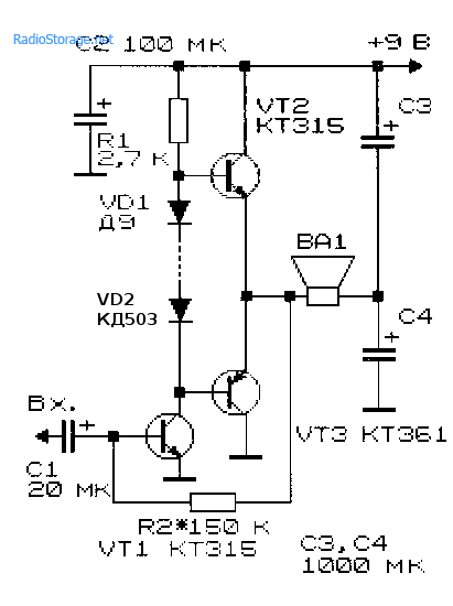
Rice. 11. A simple two-stage ULF for a microphone (low noise level, high gain).

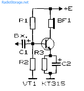
Rice. 12. Two-stage low-frequency amplifier based on KT315 transistors.

Rice. 13. Two-stage low-frequency amplifier based on KT315 transistors - option 2.
The microphone amplifier (Fig. 11) is characterized low level intrinsic noise and high gain [MK 5/83-XIV]. An electrodynamic type microphone was used as the BM1 microphone.
A telephone capsule can also act as a microphone. Stabilization of the operating point (initial bias based on the input transistor) of the amplifiers in fig. 11 - 13 is carried out due to the voltage drop across the emitter resistance of the second amplification stage.

Rice. 14. Two-stage ULF with a field-effect transistor.
The amplifier (Fig. 14), which has a high input resistance (about 1 MΩ), is made on a field-effect transistor VT1 (source follower) and bipolar - VT2 (with a common one).
A cascade low-frequency field-effect transistor amplifier, which also has a high input impedance, is shown in fig. 15.

Rice. 15. diagram of a simple two-stage ULF on two field-effect transistors.
ULF circuits for working with low-ohm load
Typical ULF, designed to operate on a low-resistance load and having an output power of tens of mW or more, are shown in Fig. 16, 17.

Rice. 16. A simple ULF for working with a low-resistance load.
Electrodynamic head BA1 can be connected to the output of the amplifier, as shown in fig. 16, or in the diagonal of the bridge (Fig. 17). If the power source is made of two batteries (accumulators) connected in series, the output of the BA1 head, right according to the diagram, can be connected to their midpoint directly, without capacitors C3, C4.
Rice. 17. Low-frequency amplifier circuit with the inclusion of a low-resistance load in the diagonal of the bridge.
If you need a circuit for a simple tube ULF, then such an amplifier can be assembled even on a single tube, see our electronics website in the appropriate section.
Literature: Shustov M.A. Practical Circuitry (Book 1), 2003.
Corrections in the post: in fig. 16 and 17 instead of the diode D9, a chain of diodes is installed.


